产品索引
联系我们
合作伙伴


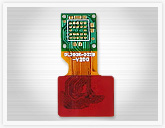
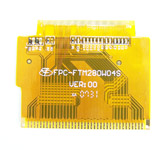
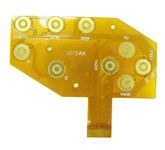
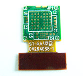
Multi-layer Board Main Application
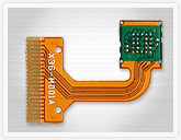
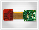
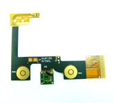
full flex pcb effect diagram
 |
 |
 |
 |
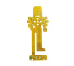
HD-OO1 |
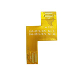
HD-002 |
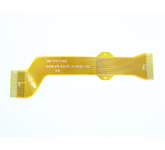
HD-003 |
HD-004 |
 |
 |
 |
 |
HD-005 |
HD-006 |
HD-007 |
HD-008 |
 |
 |
 |
 |
HD-009 |
HD-010 |
HD-011 |
HD-012 |
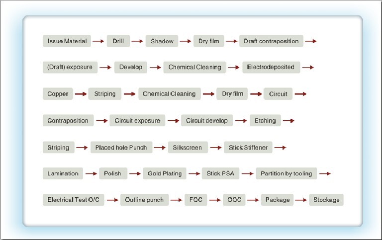
Technical Specification
Scope of products : Single-side FPC, double-side FPC, multilayer FPC, aluminum substrate, copper substrate, single-side hollowed-out FPC and double-side hollowed-out FPC
Thinnest substrate : Copper foil/PI film: 18/12.5 um 12/18um
Smallest wire width and distance : 0.05mm/0.05mm (2mil/2mil)
Smallest aperture : 0.25mm (10mil)
Resistance to flexural cracking : > 150,000 cycles
Etching tolerance : ± 0.5 mil
Tolerance for exposure and alignment : ± 0.05mm (2mil)
Tolerance for projection punching : ± 0.025mm (1mil)
Tolerance for PI film alignment : < 0.10mm (4mil)
Tolerance for reinforcing and take alignment : < 0.1mm (4mil)
Maximum processing area : 25cm × 60cm for double side; 25 cm × 10000cm for single side; 25cm × 60cm for multilayer
Forming tolerance : ± 0.05mm
Mode of surface treatment :
Electroplated guiding : 1-5u "
Chemical gilding : 1-3u "
Pure electroplating tine : 4-20u "
Chemical tin : 1-5u "
Antioxidatio n (OSP) 6-13u"
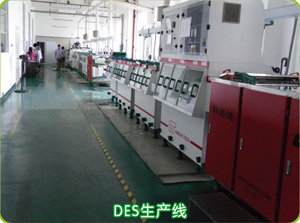
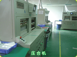
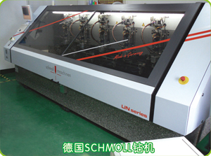
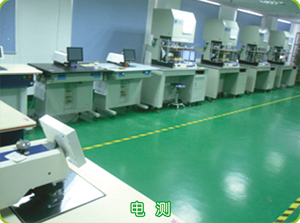
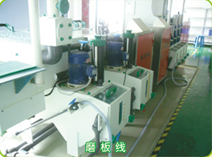
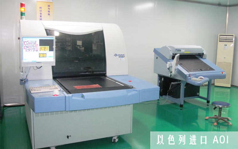
Plant
|