|
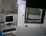
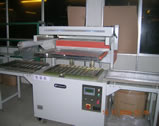
Workstation |
Content |
|
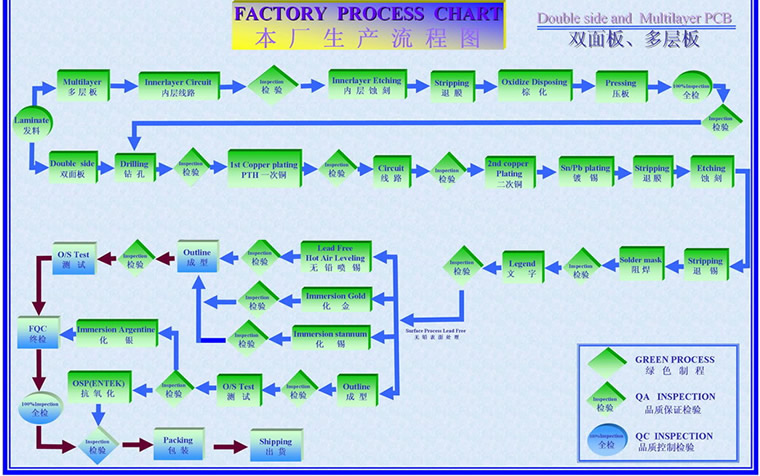
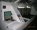
Inner layer
imaging |
Both wet and dry
film, auto-exposure machines from Japan,
horizontal etching lines from Germany, enhancing
the capability to produce min. 40μm -thick CCL
and min. width/gap 40μm/40μm. |
|
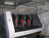
Laminating |
Leading
integrated hot and cold laminating machines from
Germany, able to process up to 40-layer PCB.
Pressing the min. thickness of 0.20mm, the max.
thickness of 5mm or more, with excellent
thickness uniformity. |
|
Mechanical
drilling |
HITACHI CNC
drilling machines to ensure the min. hole
diameter of 0.10mm with high precision. |
|
Laser drilling |
HITACHI CNC laser
drilling machines to ensure the min. hole
diameter 0.075mm, drilling speed 20,000 holes /
min or more, high-density interconnect board
producing. |
|
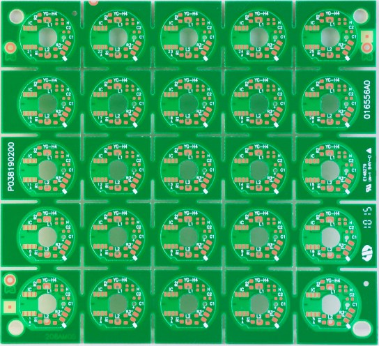
Copper plating |
Pulse plating /
Continuous vertical panel plating, special tools
for 40μm -thick CCL ,to achieve Aspect Ratio
with 20:1 and good copper distribution COV≤6%. |
|
Copper
electroplating micro via filling |
Applying selected
special chemical additives ,optimized electroplating process parameter ,together with
the appropriate electroplating equipment, to fulfill the high-end customer's requirement on
high quality of high board thickness to via
diameter ratio blind via and through via filling
capability, to ensure the reliability of the HDI
PCB. |
|
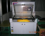
Solder mask print |
E-spray
technology, able to print over 0.1mm thin PCB,
and max.12 oz heavy copper with solder mask
thickness≥5um on trace edge. |
|
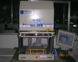
Electrical Test |
Four-terminal
tester, the min. test pad diameter at 0.1mm,
min. test resistance at 10 milliohms to ensure
quality and reliability of the HDI PCB. |
|
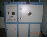
Special carbon
printing |
Special
configuration of the carbon & dielectric paste
print line, life test up to 18 million cycles to
ensure product reliabilities. |


 HD-001
  HD-002
 HD-003